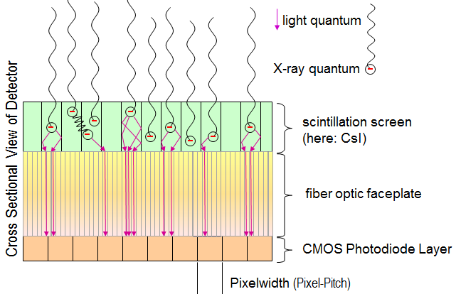
The physics behind this technology is very similar to the .
There are some advantages of CMOS technology compared to a-Si
- smaller pixel possible (cell phone cameras ~1µm)
- good linearity
- higher dynamic range (with low noise electronics)
- lower image lag
- higher frame rate
- lower costs of production.
On the other hand
- CMOS structures are more sensitive to X-ray quants and have to be protected against radiation
- active ares size is limited to the size of one wafer.
As mentioned there a lot of quants pass the scintillator and hit the silicon; sometimes 20mSv could destroy already small CMOS structures where a-Si structures would outlive factor thousand and more.
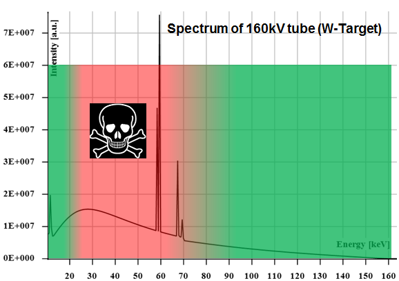
As shown in the picture above CMOS is most sensitive in the "middle area" and for NDT inspection with Tungsten targets the characteristic lines of Tungsten are inside this sensitive area.
The challenge is to block X-ray and to let light pass without getting unsharp images. Fiberoptic faceplates could do the job.
Detectors of the first generation with this technology had a (very) limited livetime. One of the reasons was the structure of the round fiber optics
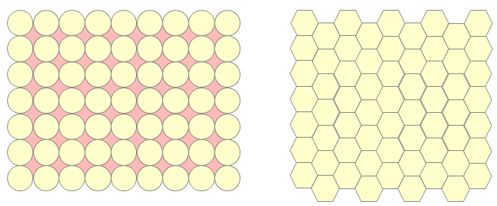
where in the areas between the fibers X-Ray could pass. Newer detectors uses hexogonal structures to avoid the "open door" for X-ray quants.
The other limiting factor is the size of the active CMOS area - it should fit into one wafer which limits the size to about 20cm*20cm (2019). Amorphous silicon is mostly used for solar cells or LCD displays or TVs where a large size is standard.